


TTM’s Leading-Edge Capabilities Deliver Reliable Advanced Technology Solutions
We are recognized as an industry-leading provider of advanced technology PCB product solutions across the networking market. Our key telecommunications manufacturing facilities provide customers with the highest levels of technology and quality, designed to support emerging optical data rates up to 3.2T and beyond.
TTM has expertise in Radio Frequency & Specialty ("RF&S") components, engineered thermal solutions, and advanced photonics packaging that set us apart from other PCB manufacturers. Our value goes beyond PCB and offers an integrated, complete solution to support your full product lifecycle.
TTM has a number of solutions and broad expertise for Networking applications

Advanced PCBs utilize cutting-edge drilling and plating technology to support high layer counts and complex designs, meeting the demands of next-generation electronics. Find out more about our PCB offerings.

All cellular devices require a network of base stations to function. The base station antennas transmit and receive RF signals, or radio waves, to and from mobile phones near the base station.
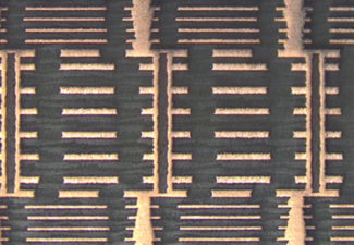
HDI PCBs capitalize on the latest technologies available to increase the functionality of PCBs using the same or less amount of area. This advancement in PCB technology is driven by the miniaturization of components and semiconductor packages that supports advanced features in revolutionary new products.
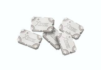
TTM manufactures a range of passive components used extensively in cellular base stations and tower mounted hardware. These products are critical signal path products that allow our customers the highest levels of performance while keeping costs down. We also offer expertise in advanced photonics packaging, engineered thermal solutions, and integrated RF solutions. Our teams have deep expertise in this area and we continue to offer differentiated products that support our innovative customer-base.
Networking Capabilities
TM Continually Invests in Capital and Talent to Meet the Needs of Networking Industries
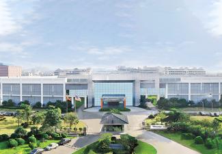
TTM Dongguan ("DMC") was established in 2001 and is best suited for advanced technology multi-layer PCB in volume.
- High layer count
- Conventional
- Hybrid & sequential structure
- HDI
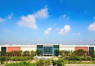
TTM Guangzhou ("GZ") is best suited for advanced technology multi-layer PCB in volume application.
- High layer count
- Conventional and advanced HDI
- Oversized line card and backplanes
- Hybrid & sequential structures
- Thermal management
TTM Penang ("PNG") is our highly advanced technology-equipped facility in Southeast Asia.
- HDI
- Highly Automated Production Lines
- Multi-layered Printed Circuit Board
- Greenfield Facility
TTM Toronto ("TOR") delivers quick-turn and ramps to low- and mid-volume under one roof.
- Quick-turn, high-mix, low- to mid-volume
- Radar and LiDAR development
- Material development; polyphenylene oxide ("PPO"), teflon
- Flex, rigid-flex
- Advanced HDI, including 3+n+3
- High layer count requiring high-performance materials, controlled impedance, back-drilling, high aspect ratio plating, VIPPO, etc.
- Seamless transfer to volume production in Asia
- Diverse laminate materials from North America and Asia Pacific