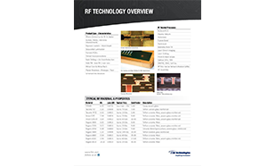
Innovative Engineering and Advanced Process Capabilities
From defense, space, and aerospace electronics, to medical devices, imaging, complex telecommunications equipment, to 5G enablement, and mmWave automotive radar, TTM supports a wide range of frequency bands (L, S, C, X, Ku, K, Ka, V, W). We have extensive experience with a wide range of low-loss laminate materials and a total of over 70 resin systems.
We are investing in research and development to provide our customers with data regarding signal integrity, materials, and high-reliability design for manufacture guidance to ensure our customers RF/Microwave reliant applications meet the needs of the market and stringent standards for quality and performance required for specific industries and reliability in the field. TTM has a dedicated Signal Integrity Lab and continues to provide industry-leading research and development in collaboration with the customers we serve.
Our broad product offerings and one-stop capabilities provide our customers with complete product lifecycle support; we have a range of engineered thermal solutions, high-current testing capabilities, low-temperature cofired ceramics ("LTCC") solutions, microwave attenuators, and so much more to ensure we add value at each stage of the product’s journey from NPI to end-of-life. Our rigorous testing and adherence to internationally recognized quality and environmental standards are just a few reasons why TTM’s teams are recognized as exceptional and why leading brands worldwide trust our advanced technology solutions.

Our Capabilities
- +/- 0.0005" (12.7um) standard tolerance on etched features for un-plated 0.5oz copper
- Selective plated up layers allowing +/- 0.0005" (12.7um) etch tolerances
- Exact registration / laser direct imaging
- Front to back registration of etched cores to +/-0.001" (25.4um)
- Hybrid dielectric material constructions
- Buried via / blind via / microvia
- Ormet paste for z-axis interconnects
- Multi-level cavity constructions
- Optical milling / drilling
- Laser routing / machining
- Sequential lamination
- Polytetrafluoroethylene ("PTFE") Fusion Bond
- Formed PCBs
- Plated edges and slots
- Mechanical back-drilling (minimal stub)
- Laser drilling (no stub)
- Laser modified controlled depth drill (mechanical drill followed by laser clean-up, no stub)
- Multi-functional hole technology allowing two nets in one hole location
- Via-In-Pad-Plated-Over ("VIPPO") with conductive and non-conductive epoxy
- Solid copper plated microvia and small mechanical drilled plated through vias
- Partial hole-fill options
- Copper coins and slugs
- HDVP & ThermalVia®
- Metal core, metal backed, and IMS
- Thermally conductive laminates
- Heatsink assembly department to laminate heatsink or interface plates to the circuit boards
- Planar Resistors / Capacitors
- Ohmega and ticer
- Screened ink resistors
- Planar capacitance materials: laminate, film based and High dielectric constant ("Dk") filled
- Circulators
- On-board circuit
- Embedded ferrites
- Embedded passive components
- Electroless Nickel, Immersion Gold ("ENIG") standard solder assemblies
- Electroless Nickel, Electroless Palladium, Immersion Gold ("ENEPIG")
- Electroless Palladium, Immersion Gold ("EPIG")
- Hard and soft wire-bondable gold
- Immersion silver
- OSP
- RF assembly of connector, surface mount component, drop-in cavity components, hand, and automated solder assembly options
- RF test centers have extensive engineering and test capabilities, including multiple Network Analyzers with combined frequency sweep coverage up to 110 GHz.
- RF and Microwave dielectric material test and characterization capabilities
- 3D laser scanning for copper foil profile analysis
- 2D Static field solvers as well as 3D full-wave simulation capability
- Custom anechoic boxes for antenna measurements
- Switch matrix capability for multiple measurements between human interaction
- Switch matrix capability for multiple measurements between human interaction


Our dedicated field applications engineers provide collaborative engineering support for the full product lifecycle, from inception to the field.
Qualifications/Certifications include; MIL-PRF-31032, AS 9100, ITAR, IPC 6012 & IPC6018, NADCAP, IATF 16949, ISO 9001, ISO 14001, ISO/IEC 17025, TL 9000-H, Bellcore Compliance, and OHSAS, as well as Automotive TS 16949 and Medical ISO 13485 certifications.

Related Resources


