


Episode #1
DC Blocking in RF Designs
Multilayer ceramic capacitors (MLCCs) are often used as DC block in RF systems to prevent the flow of DC current while allowing the passage of RF signals. In high power and high frequency applications, the choice of MLCC capacitors requires careful evaluation on several critical specifications.
Capacitance:
To block DC current and permit the desired RF signals to pass through, it is crucial to carefully select the capacitance value and allowable tolerance range based on the impedance of the circuit and frequency range of the RF system.
Equivalent Series Inductance (ESL):
Capacitors exhibit a self-resonance frequency where their equivalent series inductance (ESL) and capacitance resonate, resulting in a short circuit behavior. Typically, DC blockcapacitors are chosen with a self-resonance frequency that falls within the RF passband.
Equivalent Series Resistance (ESR):
The ESR of the capacitor should be low to minimize its impact on the overall system performance. A high ESR can lead to increased insertion loss and signal distortion.
Power handling:
The DC block capacitor should be able to handle the power levels of the RF system without degrading or failing. This is especially important in high-power RF systems.
Temperature stability:
The DC block capacitor should have good temperature stability to maintain its performance over a wide range of operating temperatures. This is particularly important in RF systems that operate in harsh environments.
Size and package:
The size and package of the DC block capacitor should be appropriate for the RF system. The capacitor should be small enough to fit in the available space.
In addition, various factors that affect reliabilities have to be carefully examined.
Mechanical stress:
High power MLCCs are often used in applications that subject them to mechanical stress, such as shock and vibration. This can cause the capacitor to crack or fail, leading to a loss of capacitance or an open circuit.
Thermal stress:
High power MLCCs can also experience thermal stress, which can cause the capacitor to fail. This can occur when the capacitor is exposed to high temperatures or rapid temperature changes, which can lead to cracking, delamination, or other forms of damage.
Design engineers need to ensure that the selected capacitor can effectively block DC current while allowing the desired RF signals to pass with minimal attenuation or loss, and that it can do so reliably over a wide range of operating conditions. It may be beneficial to implement design measures such as thermal management and shock and vibration isolation.
It is important to select high quality MLCCs from reputable manufacturers, and ensure that the specifications of the selection can meet the requirements of the operating conditions of the end applications. This task can be quite overwhelming especially when multiple sources of the component are required to enhance the resilience of the supply chain.
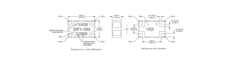
When possible, designers may also take advantage of the DC discontinuity property of adjacent component to eliminate the need for the DC block MLCC capacitor. For example, it is very common that right next to a DC block capacitor, there is a directional coupler to sample the output power. And TTM RF&S offers a family of directional couplers with DC block function built-in. These DC block directional couplers have the same package size and footprint as their conventional counterpart directional couplers. The RF performance and power rating are not compromised while offering free DC blocking. Make it an ideal substitution for the popular design arrangement of DC block MLCC capacitor followed by sampling coupler. At a bare minimum, the flexibility creates a BOM of more robust supply chain support. The other benefits are significant and can not be overlooked.
The greatest benefit comes from the physical material properties inherited in these couplers. TTM RF&S uniquely manufactures these DC block directional couplers using printed circuit board materials instead of ceramic materials. These board materials are not as brittle as ceramic materials; hence, they are more tolerable to mechanical stress and withstand shocks and vibrations much better. Furthermore, as the PCB carrier board is made of similar PCB materials, the SMT component and carrier board has much less Coefficient of Thermal Expansion (CTE) mismatch. As the component and carrier board expand and shrink at the same rate as temperature changes, there is much less thermal stress created, reducing the risk of soldering fatigue, cracking, delamination, or other forms of damage.
As TTM 100% RF tests every shipped component, the RF performance is guaranteed within the datasheet specification. The concerns related to the tolerance control of capacitance and resonance frequency in selecting MLCC capacitors can be eliminated too.
The current family (X4DB20F1-30S and X4DB40F1-30S) offers a coupling value of 30 dB from 1400MHz to 4200MHz popular 5G communication bands, and additional bands and coupling value can be added via customer requests.
It is worth mentioning, other than directional couplers, some TTMs impedance transformer components (XT0608A15005S, XT0810A15004S, XT1822A15004S, and XT2327A15002S) also have built-in DC block functions.
All of TTM’s RF&S products are available from a global team of sales partners, including RFPD, RFMW, Digi-key, and Mouser where inventory can be found to support all customer demands.
Mini-Xinger® Differential Splitters
In digital systems, clock signals are used to synchronize the timing of different components within the system. Differential signaling is a technique used for transmitting signals between two points in a system with higher noise immunity, lower EMI, and better signal integrity than single-ended signaling. One way to apply differential signaling in a clock signal is to use a differential pair of wires to transmit the clock signal. The clock signal is then encoded as a differential signal, with one wire carrying the inverted signal and the other carrying the non-inverted signal. This technique is known as differential clock signaling.

Differential clock signaling offers several advantages over single-ended signaling for clock signals. Firstly, it provides better noise immunity, which is important in high-speed digital systems where noise can cause errors in the signal. Secondly, it reduces the EMI (Electromagnetic Interference) generated by the signal, which can reduce the potential for interference with other components in the system. Finally, it provides better signal integrity, which is important for maintaining the integrity of the clock signal over long distances.
While Differential clock signaling offers several advantages for transmitting clock signals in high-speed and high-frequency applications, there are also some challenges associated with distributing these signals. For example, in some cases, it may be necessary to split a differential signal to distribute it to multiple components. This can be can be particularly challenging in high-speed designs, as the following aspects need to be carefully considered in the design:
Signal degradation:
Splitting a differential signal can result in signal degradation, which can lead to timing errors and other issues in the system. This is because the impedance of the differential signal can be affected by the splitter, resulting in reflections and signal loss.
Skew:
Differential signals rely on the accurate propagation of the inverted and non-inverted signals to maintain signal integrity. When a differential signal is split, there is a risk of skew between the two signals, which can lead to timing errors and other issues in the system.
Signal symmetry:
Differential signals require symmetry between the inverted and non-inverted signals to maintain optimal signal integrity. When a differential signal is split, it can be challenging to maintain this symmetry, which can result in signal degradation.
Crosstalk:
When a differential signal is split, there is a risk of crosstalk between the different signals. Crosstalk can result in interference and signal degradation, particularly in high-speed designs.
Layout and routing:
Proper layout and routing are critical to maintaining signal integrity in differential splitting. In most cases, crossing of the wires is inevitable and it makes the signal routing on same layer impossible. The splitter and the traces carrying the signals must be carefully designed to minimize impedance mismatches, crosstalk, and other issues that can degrade the signal.
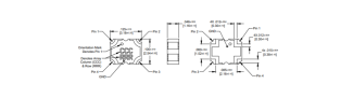
To overcome these challenges, designers can use a type of specialized components, differential splitter for such application. These components are designed to provide high-speed, low-jitter signal splitting with minimal signal degradation. These general-purpose splitters can also be used to split any differential RF/IF/LO signals in the system. With their careful layout and routing, impedance matching, and grounding, the challenges associated with differential splitting can be minimized.
TTM RF&S offers a family of differential splitters in standard 1008 size surface mountable package, covering some popular frequency bands in 5G and emerging 6G applications and additional bands can be added via customer requests.
All of TTM’s RF&S product are available from a global team of sales partners including RFPD, RFMW, Digi-key and Mouser where inventory can be found to support all customer demands.
New Product Showcase
Impedance Matched Ultra Wide Band 9200-16150 MHz 0603 Balun For TI chipsets

The X4BD130LTI is an ultra-small low profile balanced to unbalanced transformer designed specifically for Texas Instruments AFE7950 and ADC12DJ5200RF chipsets and can also be utilized with all applications called for ultra wideband coverage. The X4BD130LTI is available on tape and reel for pick and place high volume manufacturing. All of the Xinger® components are constructed from ceramic filled PTFE composites, which possess excellent electrical and mechanical stability. All parts have been subjected to rigorous Xinger® qualification testing and units are 100% RF tested.
Produced in an ENIG final finish. Key features of these baluns are: 9200-16150 MHz, 50 Ohm to 2 x50 Ohm, Ultra broadband Mil-Aero Applications, Very Low Loss – 0.7dB, Tight Amplitude and Phase Balance for class leading CMRR, Input to Output DC Isolation, Production Friendly Tape and Reel, Non-conductive Surface, RoHS Compliant and Halogen Free
Surface Mount 0402 (1mm x 0.5mm) RF Termination 0.5 Watts, 50Ω

The C05N50Z4 is a high performance ultra-small true 50Ω Aluminum Nitride (AlN) surface mount termination. The termination is designed particularly for LTE and 5G frequency bands although also offers outstanding performance over the wider frequency range from DC-6GHz and is well suited for many applications and end markets . The high power handling makes the part ideal for terminating high power 90 degree couplers and for use in microstrip circuits. The termination is also RoHS compliant and features the following key attributes: RoHS Compliant, 0.5 Watts, constructed from AlN Ceramic, Non-Nichrome Resistive Element, Low VSWR and is 100% RF Tested.
All new 3.18mm x 2.54mm “ATTO” Hybrid and Directional Couplers
The all new family of “ATTO” low profile, high performance 3dB hybrid quadrature (90 degree) and Directional couplers in a new easy to use, manufacturing friendly surface mount package. It is designed particularly for application covering 1.7GHz to 6.3GHz wireless communication frequencies. These couplers can be used for signal splitting or combining in balanced amplifiers and Doherty power amplifiers, as well as in power detection where low insertion loss and tight amplitude and phase balance control are required.
Parts have been subjected to rigorous Xinger® qualification testing and they are manufactured using materials with coefficients of thermal expansion (CTE) compatible with common substrates such as FR4, RF-35, RO4350 and polyimide. Produced with 6 of 6 RoHS compliant tin immersion finish. Key features of these tiny yet powerful couplers are: Very Low Loss, Xinger® package is production friendly, Tight Coupling, High Directivity, Tape and Reel and Lead Free.
Comprehensive 0603 3dB Hybrid, Directional coupler and Balun release update
Looking for something more?
Talk to our RF&S Specialist directly
