


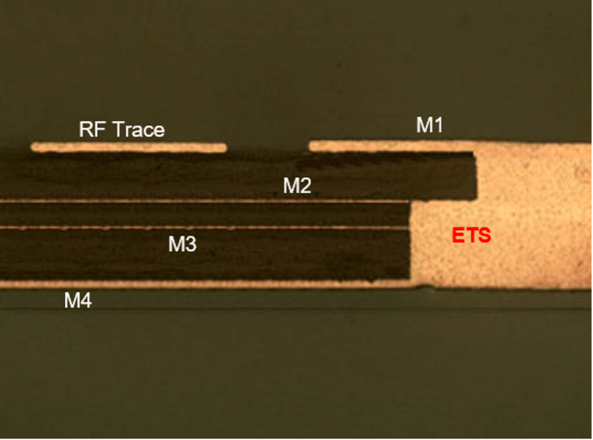
Engineered Thermal Solutions (ETS) is a unique plating process to create solid copper features for heat transfer through or across a Printed Circuit Board (PCB) utilizing standard PCB manufacturing equipment. ETS has been optimized to maximize heat transfer through thin PCBs with excellent flatness and electrical ground connectivity. It was developed to combine the individual benefits of existing PCB heat transfer solutions Coins. Thermal Via’s, without the common drawbacks of these traditional approaches and the added bonus of nontraditional shapes and can create “T” shapes for greater heat dissipation.
ETS has achieved the thermal performance of a coin with the electrical performance of a thermal via farm and the flatness of a standard PCB.
Component temperature is a directly related to performance and reliability. Everything has a Maximum Operating Temperature (MOT). When MOT is exceeded as a minimum performance is degraded and worst case is component failure. Please remember that:
- Loss increases with temperature, therefore performance decreases with increased temperature
- Increased temperature during thermal cycling increase thermal stress which increases fatigue failure
- Failure rates increase exponentially with temperature
Why is component temperature increasing?
- System densities are increasing
- Component power is increasing
- Component size is decreasing
- System heat sink temperature is increasing
The result is increased Component Thermal Density. Thermal density is dissipated power divided by area for heat dissipation. Advancements in manufacturing enable components to be made smaller and more powerful. These advancements result in increased thermal density. Additionally cost reduction efforts are driving system heat sink temperatures to increase. Examples: changing from air condition Base Station or Server Farms to ambient air cooled.
Thermodynamics Background: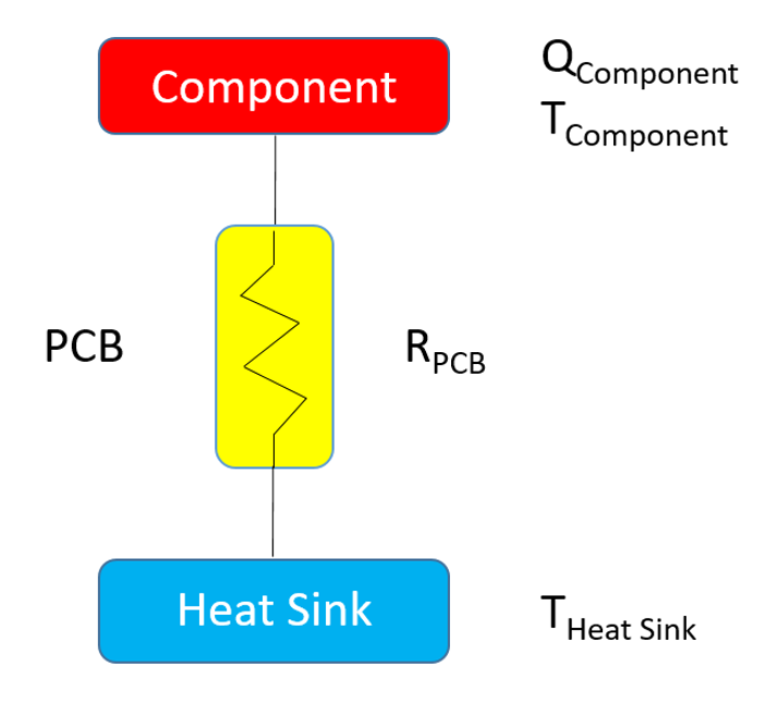
Q=dT/R
Where:
Q: Dissipated Power (W)
dT: Temperature Delta (Co)
dT = Tcomponent – THeat_Sink
R: Thermal Resistance (Co/W)
Solving for Component Temperature:
TComponent = THeat_Sink + QComponent x RPCB
Typically THeat_Sink is predefine / fixed and cannot be changed. Therefore if a component is operating above its MOT, you have two options. The first is to de-rate the component by reducing power to reduce QComponent, this is a very unpopular option. The second is to reduce RPCB.
RPCB is the resistance of the PCB to heat flow through it.
How do we reduce RPCB? The traditional methods to reduce thermal resistance through a PCB include thermal via farm, high thermal conductivity dielectric materials, coin and having a cut-out in the PCB and flange mounting the component directly to the heat sink.
A Thermal Via Farm is a dense array of Plated Through Holes under the component. Drill and plating PTHs is a routine PCB manufacturing process that is simple and low cost. Unfortunately, the PTHs must be plugged to prevent solder wicking when the component is soldered on a thermal via farm. This increases cost and process risk. Thermal via farms provide a reduction in thermal resistance compared to a bare PCB but are rarely sufficient to meet the requirements of new high power density components.
Typical PCB dielectric materials have a thermal conductivity in the range of 0.15W/mK to 0.75W/mK. High Thermal Conductivity dielectric materials range from 1 W/mK to 3 W/mK. These materials are a good option when the heat is distributed over a large percentage of the PCB. However, they are expensive and provide minimal heat transfer improvement for localized heat loads like surface mount components.
Thermal coins are pressed or laminated into cutouts in the PCB. They provide a direct metal thermal path through the PCB for heat transfer. They have very good thermal performance but they are expensive and have poor coplanarity to the PCB surface which complicates assembly of surface mount components. Additionally since they are a secondary piece, the electrical signal path to ground is longer which degrades high speed digital and RF performance.
Cutouts in the PCB and mounting the component directly on the heat sink has the best thermal performance. It also is the most labor intensive to assemble and has the longest signal path to PCB ground degrading high speed digital and RF performance.
ETS is a new heat transfer solution that combines the benefits of existing solutions without the drawbacks. It has the thermal performance of a coin with the electrical performance of a thermal via farm and the flatness of a standard PCB.
ETS Benefits
- Heat Transfer –
- High thermal conductivity > 350W/mK
- Can be irregular shapes to match the footprint of a component
- Can be small features
- Can be T-Shape, larger on the bottom to facilitate heat spreading
- Can be connected to internal ground layers which improves heat spreading
- Coplanar to PCB bottom surface
- No gap to fill with Thermal Interface Material
- Coplanar to PCB top surface
- Does not trap flux
- Electrical
- Directly connected to PCB metal layers
- No gap to ground
- No additional tolerance variation
- No deformation from press fit coins
- Not floating
- Short electrical signal path length
- Critical for high speed digital and RF applications
- Directly connected to PCB metal layers
- Manufacturing
- Utilizes standard PCB manufacturing equipment
- No new equipment required
- Ideal for Automated SMT assembly
- Works with thin PCBs
- Coplanar to PCB top surface
- Reduce tolerance for component attachment
- Does not trap flux
- Utilizes standard PCB manufacturing equipment
Looking for something more?
