


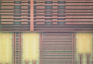
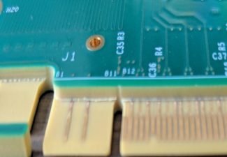
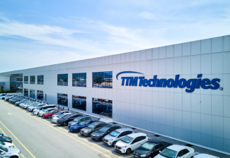
迅达提供关键印刷电路板技术以支持数据中心计算应用
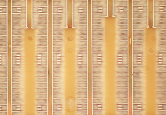
支持更多进阶计算机的能力
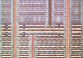
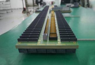
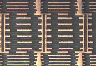
除了上述服务外,迅达提供全生命周期支持以及广泛的印刷电路板、射频/微波和工程解决方案。我们还为支持先进的数据中心计算客户提供的其他能力,包括:
- 超高纵横比
- 过孔填充
- 50 层以上
- 从原型到批量生产的无缝过渡
- 用于高速性能的先进材料和工艺
- 快速交付
迅达多伦多在同一厂区内实现提供快速周转和低到中批量生产。
- 快速周转、高混合、低到中批量生产
- 雷达和 LiDAR 开发
- 材料开发;聚苯氧化物、聚四氟乙烯 (teflon)
- 软板、软硬结合板
- 先进高密度互连,包括 3+n+3
- 需要高性能材料、控制阻抗、背钻、高 纵横比电镀、焊盘内过孔填充并电镀封孔技术 ("VIPPO") 等的高层数
- 无缝转移到亚洲批量生产
- 来自北美和亚太地区的多种层压材料